What this QDR IV SRAM brings to a high-throughput design
It is designed for applications that demand sustained read and write bandwidth with no dead cycles between bus turns — think network switch buffers, test-and-measurement acquisition memory, and high-end compute accelerators where the memory interface is the bottleneck. The 667 MHz clock rate on a QDR IV interface delivers four data words per clock cycle (two reads and two writes), effectively quadrupling the throughput compared to a single-data-rate SRAM at the same frequency. This is a part selected when a DDR3 or RLDRAM cannot match the random-access latency profile needed for look-up tables or flow-control state.
The 1.26 V to 1.34 V supply range is a dedicated core rail that should be clean and well-decoupled.
Package and physical integration
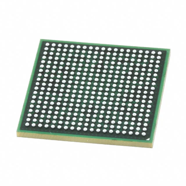
Housed in a 361-ball FCBGA (21×21 mm footprint) with a surface-mount interface. The fine-pitch BGA requires controlled impedance routing for the parallel bus and adequate decoupling capacitance distributed across the ball field — a 4-layer or 6-layer PCB is typical. The Tray shipping medium is standard for BGA devices; no reel option is listed.
This removes the last-time-buy urgency for new designs.