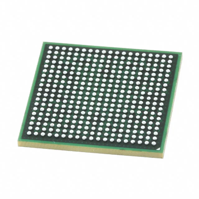
Infineon Technologies CY7C4042KV13-933FCXC — Memory (DRAM / SRAM / Flash / EEPROM)

Infineon CY7C4042KV13-933FCXC QDR IV SRAM, 72 Mbit, 933 MHz

MPNCY7C4042KV13-933FCXC
Active

Infineon Technologies CY7C4042KV13-933FCXC, synchronous QDR IV SRAM, 72 Mbit (2M x 36), 933 MHz clock, 1.26 V to 1.34 V supply, 361-FCBGA (21x21 mm), 0°C to 70°C, tray.

$241.6625Ref. price · indicative, final on quote
Sourced new & surplus through independent channelsAuthenticity-screened · ESD-safe packingListing updated Aug 2026

Specifications

CY7C4042KV13-933FCXC specifications
ParameterValue
Memory typeVolatile
MountingSurface Mount
Voltage1.26V ~ 1.34V
Frequency933 MHz
Memory interfaceParallel
Operating temperature0°C ~ 70°C (TA)
PackageTray
TechnologySRAM - Synchronous, QDR IV
Memory size72Mbit
Memory formatSRAM
Case361-BBGA, FCBGA
Memory organization2M x 36

Product details

72 Mbit QDR IV — bandwidth ceiling for the data plane

The CY7C4042KV13-933FCXC: This is a 72 Mbit synchronous SRAM organized 2M x 36, using the QDR IV architecture — a double-data-rate interface that transfers data on both clock edges, delivering a peak bandwidth of 933 MHz x 36 bits per edge. The 36-bit data bus width suits systems that need a 72-bit ECC word (two devices) or a single 36-bit datapath without parity overhead.

933 MHz clock — signal-integrity budget

At 933 MHz the parallel interface demands controlled-impedance routing, matched trace lengths, and a low-inductance decoupling network within the 361-FCBGA (21x21 mm) footprint. The supply rail tolerance is tight — 1.26 V to 1.34 V — so the board regulator must hold regulation within 40 mV under the transient load of the QDR IV I/O bank.

Frequently asked questions

What is the memory organization and interface of the CY7C4042KV13-933FCXC?

Organized 2M x 36 with a parallel QDR IV interface running at 933 MHz clock, giving a 36-bit double-data-rate bus.