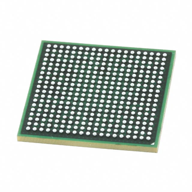
72Mbit QDR-IV SRAM for high-throughput memory subsystems
The CY7C4042KV13-106FCXC is a 72Mbit Quad Data Rate IV synchronous SRAM organized as 2M x 36 bits, clocked at 1.066 GHz. This places it in the class of high-bandwidth memory used in network packet buffers, search engines, and compute accelerator local storage where the parallel QDR-IV bus delivers four data words per clock cycle on independent read and write ports.
1.066 GHz clock and the QDR-IV bus architecture
At 1.066 GHz, the QDR-IV interface transfers data at 2.133 Gbps per pin on the read and write ports simultaneously — the effective memory bandwidth is 4.266 Gbps per DQ pin. The parallel interface means the address and control buses run at the same clock rate, so the PCB trace-length matching across the full 36-bit data bus and the address/control group must hold within a few picoseconds of skew to close timing at the controller. The core supply tolerance is tight: 1.26 V to 1.34 V. A 1.3 V nominal rail with ±3% regulation is required — a standard 1.2 V or 1.5 V rail will not hold the core within spec.
361-FCBGA package — board integration and thermal management
The package is surface-mount only and requires a multi-layer PCB with a solid ground plane under the BGA footprint. The thermal pad at the centre of the package should be connected to an inner-layer copper pour for heat spreading — the 1.066 GHz core dissipates enough that a bare BGA without a thermal via array under the die shadow will exceed the 70°C ambient limit in a confined enclosure.