72 Mbit QDR IV SRAM at 933 MHz — what the clock rate means for the bus
The CY7C4022KV13-933FCXI: The 933 MHz clock rate is the defining performance parameter: each clock edge transfers two data words (double-data-rate), giving an effective data rate of 1.866 G transfers per second per pin. That throughput targets high-bandwidth buffer applications — network switch look-up tables, traffic managers, and high-speed data acquisition — where the memory must keep pace with a 100 G or 400 G line rate without inserting wait states. The QDR IV interface separates read and write data buses, eliminating bus-turnaround dead cycles that plague common-I/O SRAMs.
1.26 V to 1.34 V supply — tight rail tolerance
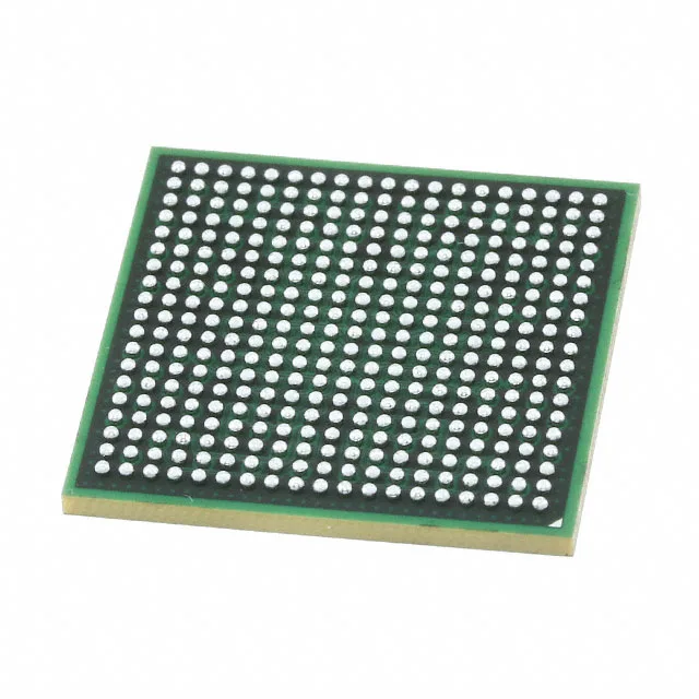
The supply range is 1.26 V to 1.34 V, a 1.3 V nominal with only ±40 mV tolerance. The board designer needs a dedicated low-noise regulator — a switching converter with <10 mV ripple or a low-dropout linear regulator — placed close to the device. Any excursion outside this window during a read or write cycle risks data corruption. The 361-FCBGA package (21x21 mm) has a central array of supply and ground balls; the layout should mirror the recommended decoupling capacitor pattern from the datasheet, with multiple 100 nF and 1 µF ceramics per quadrant.
For rework, a preheat profile that keeps the entire board above 150°C for 60–90 seconds reduces the risk of solder-joint cracking under the BGA.
The base product number CY7C4022 covers a family of density and speed variants; if a future design needs a different density or a lower speed bin, the same footprint and interface apply across the family.