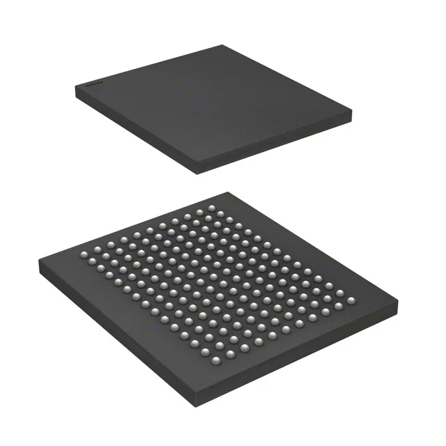
The Infineon CY7C2670KV18-550BZXI is a 144 Mbit synchronous SRAM organised as 4M x 36, using a DDR II+ (Double Data Rate II+) interface that clocks at 550 MHz. That clock rate means the memory delivers two data transfers per clock cycle on both read and write, effectively doubling the bus throughput compared to a single-data-rate part at the same frequency. For a system architect, this part fits designs that need high-bandwidth, low-latency SRAM — typically network packet buffers, telecom line cards, or high-end test equipment where the SRAM's deterministic access time beats DRAM refresh overhead.
165-ball FBGA — rework and layout considerations
The package is a 165-ball FBGA (15x17 mm body). For the PCB layout engineer, that pitch is dense enough to require micro-vias or at least a fine-line fanout between balls.
In a cold-start scenario at -40°C and 1.7 V, the PLL lock time may stretch — budget a few hundred microseconds in the power-on sequence before issuing the first read command.
For the BOM cost engineer, this removes the single-source risk flag that comes with NRND or EOL parts. The base product number is CY7C2670 — any future speed-grade or package variant will share that base, so a second-source or drop-in alternate would need to match the 165-FBGA footprint and the 550 MHz speed bin.