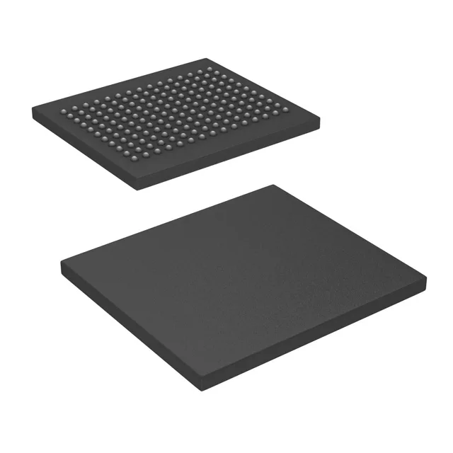
144 Mbit QDR II+ synchronous SRAM at 550 MHz — what this buys you
The 550 MHz clock rate gives back-to-back read and write transactions on separate I/O ports every cycle, which is the whole point of the QDR (Quad Data Rate) family — no bus-turnaround dead cycles. This part lives in high-bandwidth, low-latency memory slots where DDR SDRAM's burst overhead or refresh cycles are unacceptable: network switch lookup tables, TCAM companions, packet buffers, and L3 cache in custom ASIC/FPGA designs.
550 MHz clock — timing closure and signal integrity
At 550 MHz the clock period is roughly 1.8 ns. The QDR II+ architecture splits the data bus into separate read and write ports, so the controller sees a clean DDR data eye on each port without the bus-turnaround penalty that cuts effective throughput on common-I/O SRAMs. The 165-FBGA (15x17 mm) package keeps trace lengths short, but the fine ball pitch demands microvia fanout and controlled-impedance routing on at least four signal layers. Budget for series termination close to the SRAM balls — the edge rates are fast enough that unterminated stubs produce noticeable ringing above 400 MHz.
Listed as Active by Infineon.