Memory map and bus performance
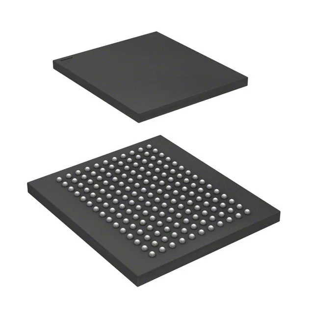
The CY7C2644KV18-300BZI is a 144Mbit QDR II+ synchronous SRAM organized as 4M x 36. The 36-bit data word is a single-cycle read or write on the rising and falling edges of the clock — QDR II+ architecture delivers two data transfers per clock cycle, so the 300 MHz clock yields a 600 MT/s data rate per I/O pin. At 300 MHz, the read-to-write turnaround is one clock cycle. The burst length is fixed at 4, and the device supports both single-address and interleaved burst sequences. The parallel memory interface means the address and control lines are shared across the 36-bit data bus — layout must match the trace-length skew budget for the full 300 MHz timing window.
Supply rails and temperature grade
Core supply is 1.7V to 1.9V — a 1.8V nominal rail with ±5.5% tolerance.
Sourcing posture
The CY7C2644KV18-300BZI is sourced through independent distribution channels.