144 Mbit QDR II+ at 333 MHz — what the clock rate buys you
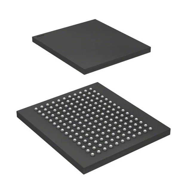
The CY7C2642KV18-333BZXC is a 144 Mbit synchronous SRAM organized as 8M x 18, clocked at 333 MHz on a QDR II+ architecture with a parallel interface. At that clock rate, the double-data-rate bus delivers 666 million transactions per second on each of the read and write ports — the effective bandwidth is what makes this part a fit for high-throughput lookup tables and buffer memories in network switches, search engines, and packet processors. The 1.7 V to 1.9 V core supply is tighter than a standard 1.8 V rail tolerance — the board designer should budget a dedicated regulator with ±3 % accuracy or better, not a shared 1.8 V plane that droops under load.
Package and board-fit — 165-ball FBGA
The 15x17 mm body fits a standard 4- or 6-layer PCB; the inner balls route out on the inner layers, so the layout engineer should plan for at least two signal layers under the package. Supplied in tray format, not tape-and-reel — the pick-and-place feeder setup differs, and the tray quantity per reel is lower, so volume assembly houses need to confirm the feeder changeover cost against the BOM quantity.
Temperature grade and deployment envelope
This part is intended for indoor, temperature-controlled environments — server rooms, central offices, and lab-grade instrumentation. It is not specified for -40°C startup or 85°C+ ambient, so an outdoor base-station or automotive design would need the industrial-temperature variant of this family. Lifecycle status is active — Infineon still produces this part.