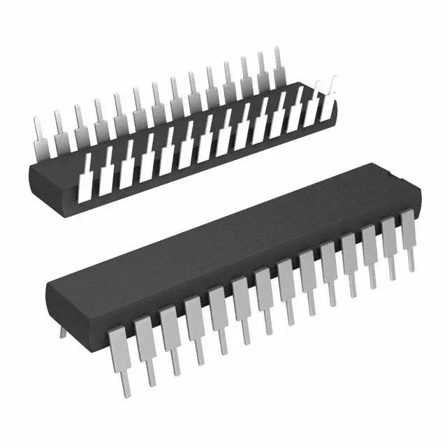
The Infineon CY7C199CN-25PXC is a 256Kbit asynchronous SRAM organized as 32K x 8 bits, with a 25 ns access time. Typical applications include cache buffers, scratchpad memory, and configuration storage in embedded controllers, telecom line cards, and industrial test equipment where a fast, simple memory interface is needed without the complexity of DRAM refresh or serial latency.
The 25 ns access time means the SRAM presents valid data within 25 ns of the address being stable. For a system running a 20 MHz bus (50 ns cycle), this leaves 25 ns of setup margin before the next clock edge — enough for most 8-bit and 16-bit microcontrollers without wait states.
5V-only supply — not a 3.3V drop-in
This part operates from 4.5V to 5.5V, so it cannot be used directly in a 3.3V system without level shifters on address, data, and control lines. The 5V supply rail also means the I/O levels are TTL-compatible at the input thresholds but swing rail-to-rail on outputs — check the host's input tolerance before connecting to a 3.3V controller.
28-PDIP through-hole — legacy footprint, socket-friendly
The 28-pin PDIP (0.300" body width) is a standard through-hole package that fits sockets or can be soldered directly into plated through-holes. For rework and prototyping, this is the easiest package to handle — no hot-air, no stencil. The 0.100" pitch matches breadboard and perfboard layouts, which is useful for repair and retrofit work on older equipment.