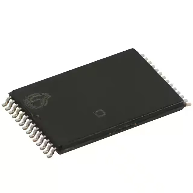
Infineon Technologies CY7C199CN-15ZXCT — Memory (DRAM / SRAM / Flash / EEPROM)

Infineon CY7C199CN-15ZXCT 256Kbit Async SRAM, 15 ns

MPNCY7C199CN-15ZXCT
Obsolete

Infineon Technologies CY7C199CN-15ZXCT asynchronous SRAM, 256Kbit (32K x 8), 15 ns access time, 4.5V-5.5V, 0°C-70°C, 28-TSSOP, Tape & Reel.

Sourced new & surplus through independent channelsAuthenticity-screened · ESD-safe packingListing updated Jul 2026

Specifications

CY7C199CN-15ZXCT specifications
ParameterValue
Memory typeVolatile
MountingSurface Mount
Voltage4.5V ~ 5.5V
Memory interfaceParallel
Operating temperature0°C~70°C(TA)
PackageTape & Reel (TR)
TechnologySRAM - Asynchronous
Access time15 ns
Memory size256Kbit
Memory formatSRAM
Case28-TSSOP (0.465\", 11.80mm Width)
Memory organization32K x 8
Write cycle time - word, page15ns

Product details

Memory density and bus timing for legacy 5V parallel designs

The CY7C199CN-15ZXCT is a 256Kbit asynchronous SRAM organized as 32K x 8 bits, with a 15 ns access time that sets the ceiling for read-cycle timing on a parallel bus. The 15 ns access time means the memory can complete a read within 15 ns of the address being valid. For a system with a 33 MHz bus clock (30 ns period), this leaves 15 ns of margin after the address settles before the data must be latched — adequate for most asynchronous bus controllers, but tight if the controller adds its own propagation delay.

No stock-holding claim is made here.

Package and board-fit for the 28-TSSOP footprint

The supplier device package is designated 28-TSOP I — the two terms refer to the same mechanical outline. Tape & Reel packaging supports pick-and-place reflow soldering.

Frequently asked questions

What is the closest pin-compatible alternative to CY7C199CN-15ZXCT?

No official pin-compatible successor or cross-reference is recorded from Infineon for this order code. A functional replacement would require a 256Kbit (32K x 8) asynchronous SRAM in a 28-TSSOP package with a 15 ns or faster access time and a 5V ±10% supply — but the pinout must be verified against the target PCB layout before substitution.