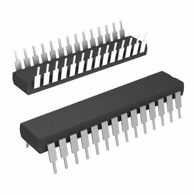
256Kbit parallel SRAM in a hand-solderable DIP
The CY7C199CN-15PXC is a 256Kbit asynchronous SRAM organized as 32K x 8 bits, with a 15 ns access time that matches the write cycle time — meaning the bus master can read or write any location in a single 15 ns window without wait states. It runs on a 4.5V to 5.5V supply rail, so it drops straight into legacy 5V logic systems or retrofits older CPU boards without a level translator. The 28-pin DIP package (0.300" body width) is through-hole — you can hand-solder it on a perfboard or socket it for a breadboard prototype, which makes it a favourite for hobbyists repairing vintage computers or building 8-bit retro systems.
What the 15 ns access time means for your bus
If your processor runs at 40 MHz (25 ns cycle), the 15 ns access leaves 10 ns for address decoding, bus transceivers, and setup time at the CPU, which is tight but workable with fast logic. The write cycle time is also 15 ns, so byte-wide writes complete at the same speed as reads — no asymmetric penalty when the code mixes load and store operations. The parallel interface (32 data lines multiplexed as 8-bit bytes across the address space) connects directly to a microcontroller's external bus or an FPGA's SRAM controller without a serial-to-parallel conversion delay.
Temperature grade and board-fit notes
The 28-pin DIP footprint is 0.300" (7.62 mm) wide with 0.100" (2.54 mm) pin pitch — a standard socket or solder pads on 0.1" grid protoboard fit without layout changes. Supply decoupling: place a 0.1 µF ceramic capacitor as close as possible to pins 28 (Vcc) and 14 (GND) — the 15 ns edge rates draw transient current that a distant cap cannot supply fast enough.