256Kbit async SRAM for 5 V parallel bus — 20 ns access sets the read-cycle budget
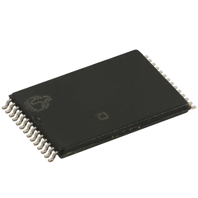
The CY7C199C-20ZI: The 20 ns access time is the address-to-data-valid delay — it sets the minimum read-cycle time on a 5 V parallel bus. A 20 ns access means the bus controller must hold the address stable for at least 20 ns before latching the data; any faster bus cycle misses the data window.
Obsolete — no official successor on record
Infineon lists the CY7C199C-20ZI as Obsolete. No official replacement part number has been published. The 28-TSOP I footprint and 5 V ±10% supply are the constraints for any functional replacement; a pin-compatible drop-in from another manufacturer would need to match the 32K x 8 organization, 20 ns or faster access, and the same package outline.
Timing parameters that govern bus fit
The 20 ns write cycle time (word, page) matches the read access time — the write pulse width (tWP) and address setup-to-write-end (tAW) are the critical parameters for bus-turnaround timing on a shared address/data bus. The asynchronous interface means no clock, no refresh overhead; the part is ready to read or write as soon as the address and chip-select are stable.
Package and footprint — 28-TSOP I, 11.80 mm body width
The 28-TSOP I (0.465-inch / 11.80 mm body width) uses a 1.27 mm pitch, standard for TSOP I SRAMs in this density. The surface-mount footprint is shared with other 28-pin TSOP I asynchronous SRAMs from the same era — a replacement candidate must match the 11.80 mm body width and 1.27 mm lead pitch to fit the existing PCB layout without a board spin.