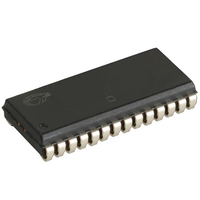
Infineon Technologies CY7C199C-20VXC — Memory (DRAM / SRAM / Flash / EEPROM)

CY7C199C-20VXC Infineon 256Kbit Async SRAM, 20 ns, SOJ-28

MPNCY7C199C-20VXC
Obsolete

Infineon CY7C199C-20VXC, 256Kbit asynchronous SRAM, 32K x 8 organization, 20 ns access time, parallel interface, 4.5V-5.5V supply, 0°C to 70°C, 28-SOJ package.

Sourced new & surplus through independent channelsAuthenticity-screened · ESD-safe packingListing updated Jul 2026

Specifications

CY7C199C-20VXC specifications
ParameterValue
Memory typeVolatile
MountingSurface Mount
Voltage4.5V ~ 5.5V
Memory interfaceParallel
Operating temperature0°C ~ 70°C (TA)
PackageBag
TechnologySRAM - Asynchronous
Access time20 ns
Memory size256Kbit
Memory formatSRAM
Case28-BSOJ (0.300\", 7.62mm Width)
Memory organization32K x 8
Write cycle time - word, page20ns

Product details

20 ns async SRAM for legacy 5 V bus systems

The CY7C199C-20VXC: Housed in a 28-SOJ surface-mount package, this part is a drop-in for legacy 5 V processor and DSP designs that need fast, byte-wide scratchpad or look-up table memory without the overhead of a synchronous clock.

Obsolete — plan for a last-time buy or surplus channel

Infineon lists the CY7C199C-20VXC as Obsolete. For production builds, this means new- and surplus-stock procurement through independent distribution is the only channel. If the BOM still calls for this exact footprint and timing, secure inventory now — the surplus pool shrinks as existing stocks are consumed.

In a 5 V system with a 50 MHz bus (20 ns period), this leaves zero margin for address decoding, trace delay, and setup time at the processor — so this part is really suited to 25–33 MHz buses where you have 10–15 ns of slack.

Frequently asked questions

What is the access time of CY7C199C-20VXC?

The access time is 20 ns, which also matches the write cycle time of 20 ns. This makes it suitable for 5 V bus systems running at 25–33 MHz where timing margin is available.