20 ns access time — bus timing fit
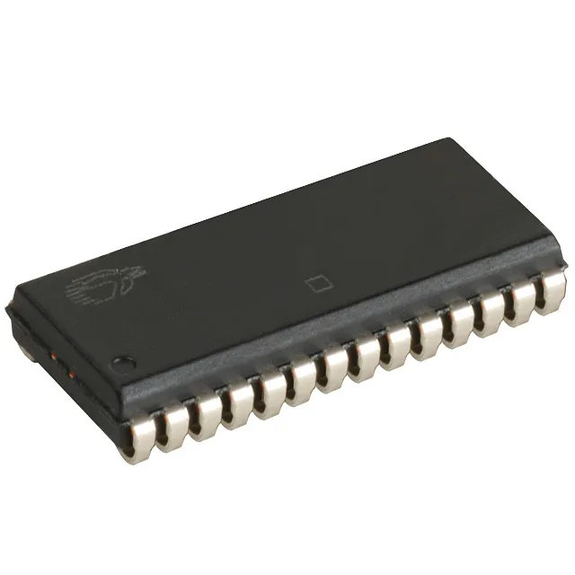
The Cypress CY7C199C-20VC is a 256Kbit asynchronous SRAM organized as 32K x 8 bits, with a 20 ns access time that determines whether it can serve a fast bus without wait states. Running on a 5V supply (4.5V to 5.5V), it uses a parallel interface and is housed in a 28-SOJ package (28-BSOJ, 0.300" width). This part targets legacy 5V logic systems — think 68K or x86 embedded boards, telecom line cards, or test equipment from the late '90s through mid-2000s where the memory bus ran at 33 MHz or slower. The 20 ns access time gives roughly a 50 MHz bus cycle headroom before wait states are needed, assuming typical address-to-data setup margins.
32K x 8 — byte-wide memory map
The 32K x 8 organization means this SRAM maps directly onto an 8-bit data bus with a 15-bit address bus (A0–A14). If your design uses a 16-bit or 32-bit bus, you will need two or four of these in parallel with a byte-lane decoder. The write cycle time matches the access time at 20 ns, so back-to-back writes run at the same speed as reads — no dead cycles for bus turnaround. That matters for designs that alternate read and write on every clock edge, like a dual-port FIFO emulation.
5V supply — not a 3.3V part
The supply range is 4.5V to 5.5V, so this SRAM is strictly a 5V-logic device. If your system runs at 3.3V, this part will not operate — the inputs will not cross the VIH threshold, and the outputs will not swing rail-to-rail. A 3.3V-compatible async SRAM like the CY7C1021 series (with a 2.7V to 3.6V range) would be the correct choice for a low-voltage bus.
If your design can tolerate a footprint change, a modern 256Kbit async SRAM in a TSOP-32 or SOIC-28 package (like the ISSI IS61LV25616AL) would be a more sustainable alternative, but that requires a board spin.