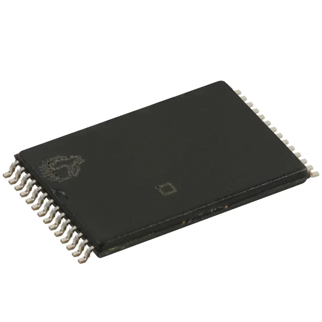
The CY7C199C-12ZXCT is a 256Kbit asynchronous SRAM organised as 32K x 8 bits, meaning it stores 32,768 words of 8 bits each — a common size for microcontroller data buffers, cache tag storage, or FPGA configuration shadow memory in legacy 5 V systems. Its 12 ns access time means the memory can complete a read or write cycle in 12 ns, which corresponds to a maximum bus speed of about 83 MHz — fast enough for many mid-range processors and DSPs from the late 1990s and early 2000s. The parallel interface uses separate address and data buses, so it connects directly to a processor's memory controller without serialisation overhead — simpler to route than a serial RAM but uses more board traces.
Supply voltage and temperature grade — design constraints
If your system runs on 3.3 V logic, you will need level translators or a separate 5 V rail for the memory. That rules out outdoor enclosures, engine bays, or unheated warehouses — the part is designed for office equipment, lab instruments, and indoor telecom racks.
Infineon lists the CY7C199C-12ZXCT as Obsolete, which means the manufacturer has stopped production and no further wafer starts or assembly runs are planned. The package is 28-TSOP I in Tape & Reel — a surface-mount footprint that is still common, so rework and replacement are straightforward if you have existing boards.