12 ns access time — keeping the bus fed
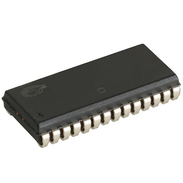
The CY7C199C-12VXI is a 256Kbit asynchronous SRAM organized as 32K x 8, built by Infineon (formerly Cypress). Its 12 ns access time means the CPU can read or write a byte every 12 ns without inserting wait states — critical for high-throughput cache or buffer memory in 5V DSP and microcontroller systems. The parallel interface is straightforward: address in, data out, chip-select and write-enable strobes.
5V supply — legacy bus compatibility
Supply range is 4.5V to 5.5V, confirming this is a 5V part. That matters when the rest of the board runs on a 5V rail — no level translation needed on the address and data lines. If your design has moved to 3.3V or lower, this part won't work without a separate 5V supply and bus translators.
The 28-SOJ package (300-mil body, 7.62 mm width) is a surface-mount footprint common on legacy industrial boards.
Infineon lists the CY7C199C-12VXI as Obsolete. No last-time-buy window remains; new production has ended. No official pin-compatible successor is recorded, so any replacement requires a footprint or timing review.