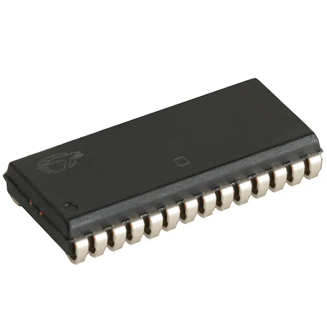
256 Kbit, 12 ns — what the access time means for fit
The CY7C199C-12VXC: Organized 32K x 8, this asynchronous SRAM delivers a 12 ns access time from address to data valid. That speed suits it for cache or scratchpad duty in legacy 5 V logic systems where a slower SRAM would insert wait states into the CPU bus cycle. The parallel interface needs no clock or refresh — it decodes the address and presents data within the 12 ns window, making it a drop-in for older DSP, microcontroller, or FPGA designs that expect a simple SRAM handshake.
5 V supply, 28-SOJ — board-fit considerations
Housed in a 28-BSOJ (0.300-inch body width, 7.62 mm), the narrow SOJ footprint matches the JEDEC standard for 28-pin SOJ SRAM. The surface-mount gull-wing leads are soldered with a standard reflow profile; no special bake or moisture sensitivity label is noted in the record. Rated for commercial temperature range 0°C to 70°C — suitable for indoor, temperature-controlled equipment. Not qualified for extended industrial or automotive ambient conditions.