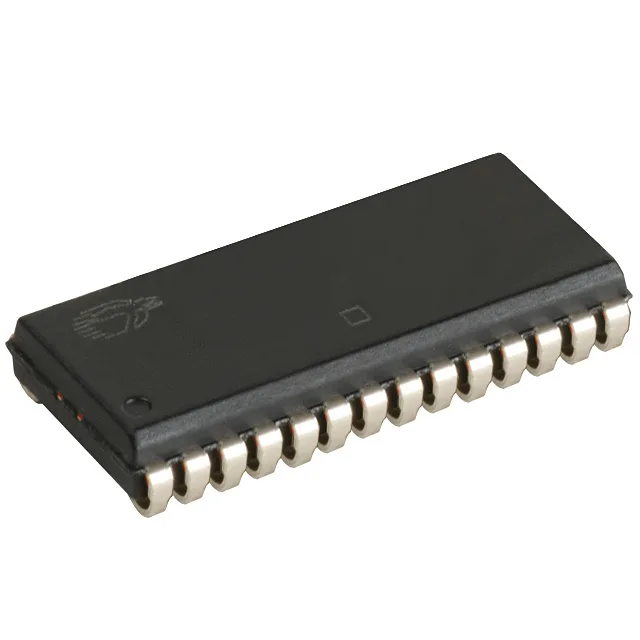
Device identity and bus-fit
The CY7C199C-12VC is a 256Kbit asynchronous SRAM organized as 32K x 8 bits, with a parallel memory interface and a 12 ns access time. The 12 ns access time sets the window the memory controller must budget for address-to-data valid — at a 33 MHz bus clock (30 ns period), the 12 ns access leaves 18 ns for controller overhead and board trace delay, which is comfortable for most legacy 5 V systems. The commercial temperature range (0°C to 70°C) suits indoor equipment with controlled ambient — think benchtop instruments, networking gear in conditioned racks, or test equipment. For extended or industrial temperature, a different suffix variant would be needed.
The J-lead footprint is less common in modern high-density designs but was a standard for mid-density SRAMs — the leads are formed under the body, saving board area compared to an SOIC. Rework requires a hot-air station with a nozzle that clears the body height; the J-leads are less accessible to a standard soldering iron tip than gull-wing leads. Supplied in Tube packaging, it is suited for manual assembly or low-volume pick-and-place where the tube feeds into a vibratory feeder or hand-load station. Tape-and-reel would be the alternate packaging for high-volume automated lines.
Lifecycle reality — obsolete, sourced to order
Sourcing is handled on a per-RFQ basis: quantities are confirmed at quote time, and the supply posture is lot-specific from surplus or broker inventory. No stock-holding or lead-time claim is made here; availability is verified when you request a quote. If your design can tolerate a board spin, a modern 3.3 V 256Kbit asynchronous SRAM in a TSOP or BGA package would be the functional migration path — but that requires a supply-voltage change and a new PCB footprint. For legacy production runs, the CY7C199C-12VC remains orderable through the channel described above.