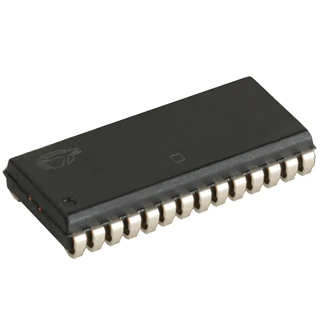
256Kbit asynchronous SRAM, 12 ns access — what the timing means for the bus
The CY7C199-12VC is a 256Kbit asynchronous SRAM organized as 32K x 8 bits, with a 12 ns access time across the full 4.5V–5.5V supply range. That 12 ns window sets the maximum read-cycle rate the host controller must respect — a 66 MHz bus with a 15 ns cycle budget has margin; an 80 MHz bus does not. The part uses a parallel interface with no clock — address changes propagate through the sense amps, and the data appears on the I/O pins within 12 ns of the address valid edge. Write cycle time is also 12 ns for word and page modes, so the read and write timing are symmetric.
Obsolete — sourcing through surplus channels
For a BOM that already uses this exact footprint (28-SOJ, 0.300-inch body width, 7.62 mm) and the 5V-only supply rail, the only drop-in path is the same order code or a verified second-source equivalent from the same base product family.
5V-only supply — not 3.3V tolerant
It is not a 3.3V device — applying 3.3V to Vcc will not guarantee correct read or write operation. The commercial temperature grade (0°C to 70°C) limits deployment to indoor, temperature-controlled environments. No industrial or automotive temperature range is specified.