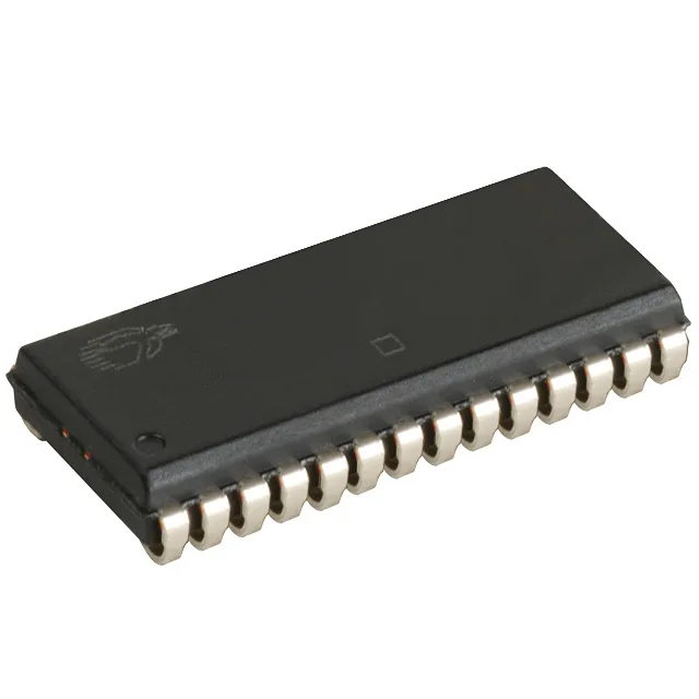
64Kbit asynchronous SRAM for 5V legacy buses
The Infineon (formerly Cypress) CY7C185-35VC is a 64Kbit asynchronous SRAM organized as 8K x 8 bits, accessed through a parallel interface with a 35 ns access time. This part is a drop-in fit for legacy 5V logic systems that need fast scratchpad memory, small look-up tables, or cache buffers — typical in older telecom line cards, industrial controllers, and test equipment that still run on 5V rails.
35 ns access time — timing margin for 8-bit buses
The 35 ns access time (and matching 35 ns write cycle) sets the bus timing window for read and write operations. In a system with a 5V 8-bit microcontroller or a CPLD memory controller running at 10–20 MHz, this gives about 15–25 ns of margin after address decode and buffer delays — enough for a single wait-state or a zero-wait-state design depending on the controller's memory timing. The parallel interface is straightforward: chip enable, output enable, and write enable control the bus, with no clock or burst logic to configure.
28-SOJ package — legacy footprint, verify board clearance
The J-lead form factor was common in the 1990s and early 2000s for SRAMs and DRAMs; it offers a smaller footprint than a DIP but requires the correct pad geometry and solder paste stencil aperture to avoid opens.
For new designs, look at the Cypress (now Infineon) CY7C1021 or CY7C1041 series in 5V or 3.3V variants — but these are different densities and packages, not pin-compatible.