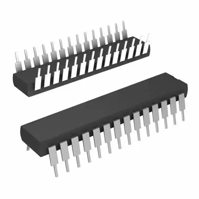
The CY7C185-20PXC: Sourcing is through independent distribution channels. Availability is lot-specific and confirmed at RFQ; pricing reflects the spot market for this end-of-life SRAM.
8K x 8 asynchronous SRAM, 20 ns access
This is a 64Kbit (8K x 8) parallel asynchronous SRAM with a 20 ns access time. The 20 ns figure means the address-to-data-valid delay — the memory returns data within 20 ns of the address being stable on the bus, which sets the cycle time for the host processor or state machine. Asynchronous operation means no clock is required; the chip select and output enable pins gate the data bus directly. This simplifies glue logic in legacy 8-bit microcontroller or DSP designs that use a separate address and data bus.
5V supply, 28-pin DIP, commercial temp
Supply voltage is 4.5V to 5.5V — a 5V nominal rail typical of legacy TTL-logic systems. Packaged in a 28-pin DIP (0.300-inch body width, 7.62 mm), through-hole mount. The supplier device package is 28-PDIP. This footprint is common on legacy CPU boards, EPROM programmers, and test equipment that use a socketed memory IC. The write cycle time is also 20 ns (word, page mode), matching the read access time — the bus timing is symmetric for read and write operations.