DDR II+ SRAM at 450 MHz — bus timing and memory map
The CY7C1668KV18-450BZXC is a 144 Mbit DDR II+ synchronous SRAM from Infineon, organized 8M words deep by 18 bits wide. The 450 MHz clock means the data bus toggles on both edges — the effective data rate is 900 MT/s per pin, so the interface timing closure at the controller side needs a clean clock tree and matched trace lengths on the 18-bit data group. Memory is organized 8M x 18 — the 18-bit word width suits applications that need a narrow but fast data path, such as a deep packet buffer or a lookup table in a networking ASIC. The 144 Mbit density fills a single-chip footprint where a 9 M x 18 or 4 M x 36 part would leave unused rows.
165-ball FBGA — board integration checklist
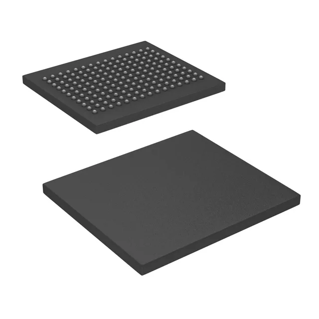
Housed in a 165-ball FBGA (15 x 17 mm body), the part uses a 0.80 mm ball pitch. The 1.7 V to 1.9 V core supply is a single rail, but the PLL and I/O buffers are sensitive to ripple — a dedicated LDO or a low-noise regulator branch on the PCB is standard practice. Decoupling should follow the layout guidelines in the Infineon application note for the QDR-II+ family. This part is not rated for industrial or automotive ambient; if your enclosure sees >70 °C or sub-zero startup, a wider-temp variant from the same family is needed.
Active lifecycle — sourcing posture
Tray packaging is standard for this BGA — suitable for prototype and low-to-mid volume builds.