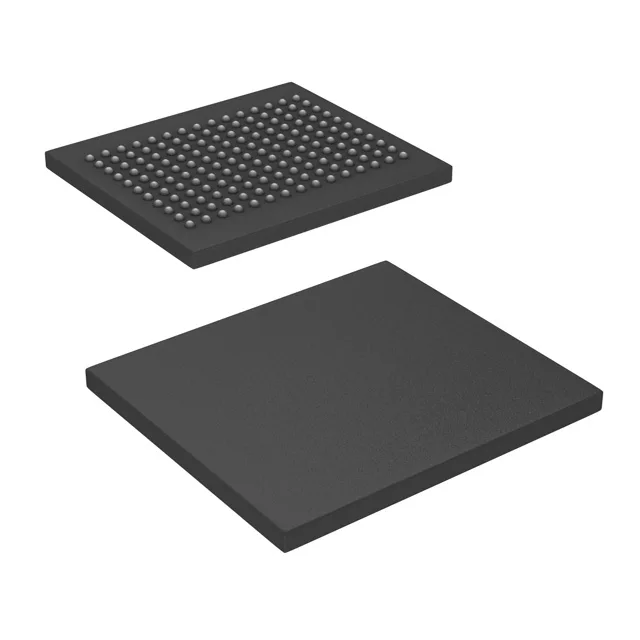
It is organized as 4M x 36 and clocked at 400 MHz, which gives it the read-write throughput needed for high-bandwidth buffer and lookup-table applications in networking, telecom, and data-acquisition systems.
400 MHz clock — what it buys the system architect
At 400 MHz, this SRAM delivers a burst rate that keeps up with high-speed packet processors and FPGA-based state machines. The QDR II+ architecture eliminates the read-write turnaround dead cycles that older synchronous SRAMs suffer, so back-to-back transactions at full clock rate are possible. For a system architect sizing the memory subsystem, the 400 MHz rating is the ceiling for the bus timing closure — the controller and PCB trace delays must fit within one clock period at that speed.
Layout engineers should budget for at least four decoupling capacitors per supply ball group, placed as close to the BGA footprint as the escape routing allows.