What this QDR II SRAM brings to a high-throughput datapath
It is organized as 16M x 9 and clocks at 250 MHz, delivering back-to-back read and write transactions on separate ports without idle cycles between direction changes.
At 250 MHz the clock period is 4 ns. The QDR II interface uses source-synchronous clocking with a separate echo clock from the SRAM, so the PCB trace-length matching between the data, address, and clock lines needs to stay within roughly ±50 ps to avoid setup/hold violations. A board designer familiar with DDR memory routing will find the layout guidelines similar, but the QDR II's independent read and write ports simplify the bus — you never pause to turn the bus around, which eases timing closure on the controller side.
No immediate supply risk, but as with any high-speed synchronous memory, securing a multi-year forecast with the distributor avoids spot-market surprises.
Package considerations for the rework bench
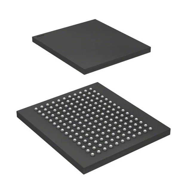
The 165-FBGA (15x17 mm) is a standard fine-pitch BGA with 1 mm ball pitch. For rework, the standard lead-free profile with a 240°C peak works; the part is MSL 3, so a bake at 125°C for 48 hours is required if the moisture-barrier bag has been open longer than the floor-life window. A bottom-side preheat at 150°C helps avoid cold-joint rework on the large ground plane under the BGA.