144 Mbit QDR II buffer — clock rate and organization
The CY7C1625KV18-250BZXC is a 144 Mbit Quad Data Rate II synchronous SRAM organized as 16M x 9. The 250 MHz clock delivers a peak data rate of 1 Gbps per I/O pin (double-data-rate on both read and write ports), making it suited for high-throughput buffer applications in network switches, routers, and telecom line cards where the QDR II architecture eliminates the read-write bus-turnaround penalty of conventional SRAM. The 9-bit-wide data bus (8 data bits plus one parity bit per word) matches the word width of common network packet processors and search engines that expect a parity lane alongside the data path.
165-ball FBGA — board integration demands
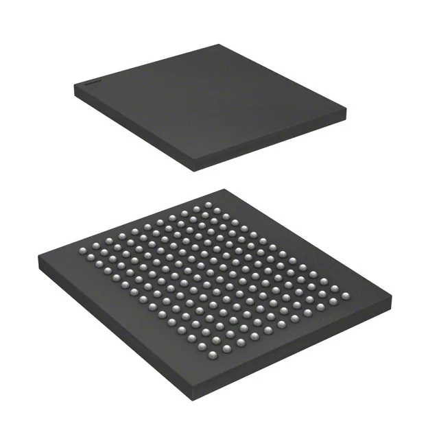
Housed in a 165-ball fine-pitch BGA (15x17 mm body, 1.0 mm ball pitch), this SRAM requires a multi-layer PCB with controlled-impedance traces for the 250 MHz clock and data lines. The 1.7V–1.9V core supply is a single 1.8 V nominal rail — no separate VDDQ supply is needed, which simplifies the power-tree design compared to earlier QDR generations that used split VDD/VDDQ.
Active lifecycle — sourcing posture
Supplied in tray packaging (standard for BGA devices in prototype and low-to-medium volume builds). For reel/tape quantities, confirm the alternate order code with your sourcing desk.