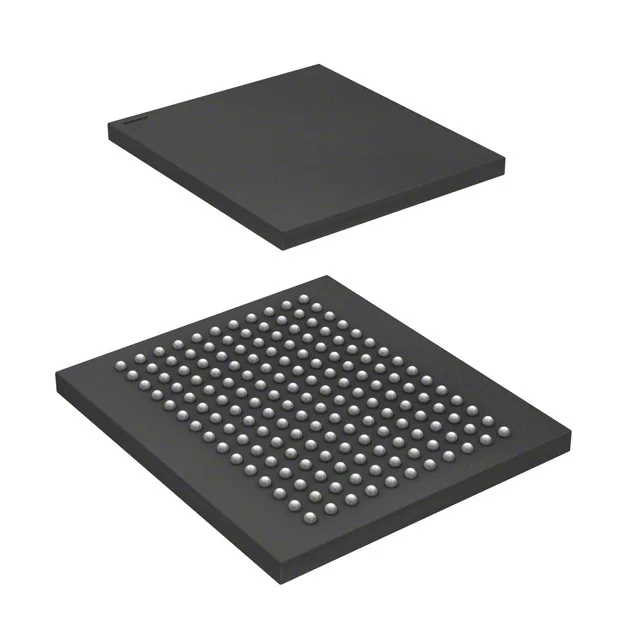
333 MHz DDR II SRAM for high-bandwidth buffer applications
The Infineon CY7C1618KV18-333BZXC is a 144Mbit synchronous DDR II SRAM organized as 8M x 18 bits, clocked at 333 MHz over a parallel interface. It operates from a 1.7V to 1.9V supply and is housed in a 165-FBGA (15x17 mm) for surface-mount assembly.
Clock frequency and memory organization — what drives the BOM fit
The 333 MHz clock rate on a DDR II interface means the SRAM delivers two data transfers per clock cycle, effectively doubling the bus throughput compared to a single-data-rate device at the same frequency. For a design that already budgets a 1.7V-1.9V core rail and a 165-ball FBGA footprint, this part slots into the memory controller's timing closure without needing a voltage translation or a larger package. The 8M x 18 organization suits 18-bit or 36-bit bus widths (two chips cascaded) commonly found in wide data-path buffers for Ethernet frame processors or FPGA-based acquisition cards.
Package and temperature — what the commercial grade tells you
If the system must survive -40°C startup or 85°C ambient, a different temperature-grade variant in the same family would be needed.