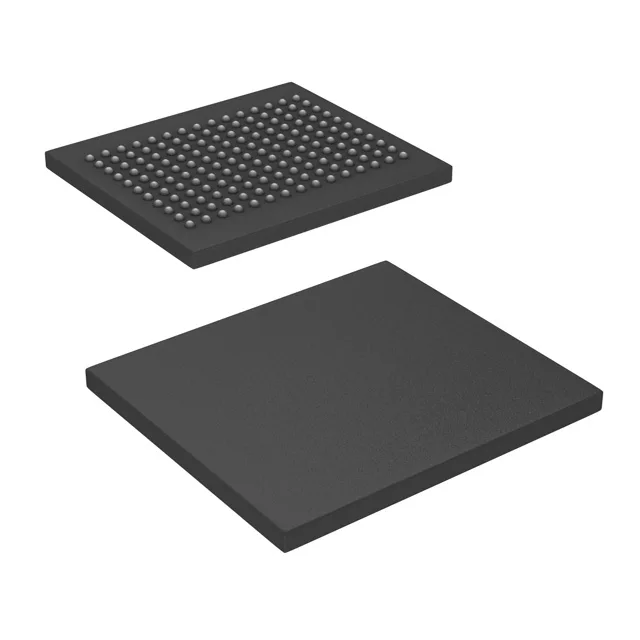
QDR II synchronous SRAM, 144 Mbit, 300 MHz — last-buy status
The CY7C1618KV18-300BZXC is a 144 Mbit QDR II synchronous SRAM organized as 4M x 36, clocked at 300 MHz, in a 165-ball FBGA (15x17 mm) package on tray. Infineon has placed this part in Last Buy status — it is not recommended for new designs, and the procurement window is finite.
Package and board integration — 165-ball FBGA
Housed in a 165-ball FBGA (15x17 mm) per the supplier device package designation, this is a fine-pitch BGA that demands a multi-layer PCB with controlled-impedance traces for the 300 MHz parallel bus. The 0.80 mm ball pitch requires careful fan-out planning — four-layer boards are marginal; six layers are typical for signal integrity at this data rate. The supply range is 1.7 V to 1.9 V — a clean 1.8 V rail with <3% ripple is expected. The core and I/O share this rail; decoupling should follow the manufacturer's layout guidelines for QDR II devices, typically one 0.1 µF MLCC per VDD ball pair plus bulk capacitance at the board edge. This part is not qualified for extended industrial or automotive thermal profiles — a heatsink is not required within this range, but airflow across the package improves reliability at the upper end.
Memory organization and interface — what the 4M x 36 means for the bus
The 4M x 36 organization means the address bus is 22 bits wide (4M = 2^22), and the data bus is 36 bits wide — a 32-bit word plus 4 parity/ECC bits per access. This suits networking and telecom line-card applications where the extra bits carry control or error-detection signals without a separate chip. QDR II (Quad Data Rate II) architecture delivers four data words per clock cycle — two on the rising edge and two on the falling edge of both the K and K# clocks. At 300 MHz, the peak data rate is 300 MHz × 4 × 36 bits = 43.2 Gbit/s (5.4 GB/s), making it suitable for high-throughput packet buffers and cache lookup tables. The memory interface is parallel — all address, data, and control signals are single-ended CMOS. This contrasts with serial memory (SPI, OPI) which uses fewer pins but has higher latency per access. The 165-ball FBGA dedicates roughly 100 balls to signal I/O; the remainder are power and ground.
Lifecycle reality — Last Buy, not active production
Infineon's official status for CY7C1618KV18-300BZXC is Last Buy. This means the manufacturer has discontinued the part and is fulfilling final orders within a defined window. After that window closes, supply is limited to existing inventory held by distributors and brokers. A functional replacement would require a board spin — the 165-FBGA footprint and 1.8 V I/O are common in the QDR II family, but any alternative must match the 4M x 36 organization and 300 MHz timing. Confirm the BOM position before committing. Sourcing is through independent distribution channels. Each lot is traceable; date-code consistency and package condition are verified before shipment. Request a quote for current availability and pricing — the Last Buy window means quantities are finite and lead times vary.