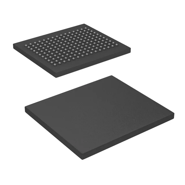
QDR II SRAM — 144 Mbit at 250 MHz
The CY7C1614KV18-250BZI is a 144 Mbit synchronous SRAM organized as 4M x 36, using the QDR II architecture with a parallel interface. The 250 MHz clock rate delivers a peak bandwidth of 18 Gbit/s on the 36-bit data bus — this is the throughput ceiling for the read-write pipeline in a networking or test-equipment buffer. The 165-ball FBGA package (15 x 17 mm body) requires a controlled-impedance board stack-up — the 0.80 mm ball pitch and the 36-bit data bus demand at least four signal layers for fan-out without via stubs on the high-speed lanes.
Active lifecycle — sourcing posture
Infineon lists the CY7C1614KV18-250BZI as Active (current production).
The 165-ball FBGA (15 x 17 mm) is a surface-mount package supplied in tray format. The 0.80 mm ball pitch and the 36-bit parallel bus require a multi-layer PCB with matched trace lengths on the data and address lines to maintain setup-and-hold margins at 250 MHz. The 1.7 V to 1.9 V supply rail should be decoupled with a 0.1 µF capacitor per supply ball pair, placed within 2 mm of the ball centroid. The FBGA's junction-to-board thermal resistance (not listed in the spec table) typically runs 15-20 °C/W for a 15x17 mm body with a 4-layer board — budget the power dissipation from the 250 MHz switching activity accordingly.