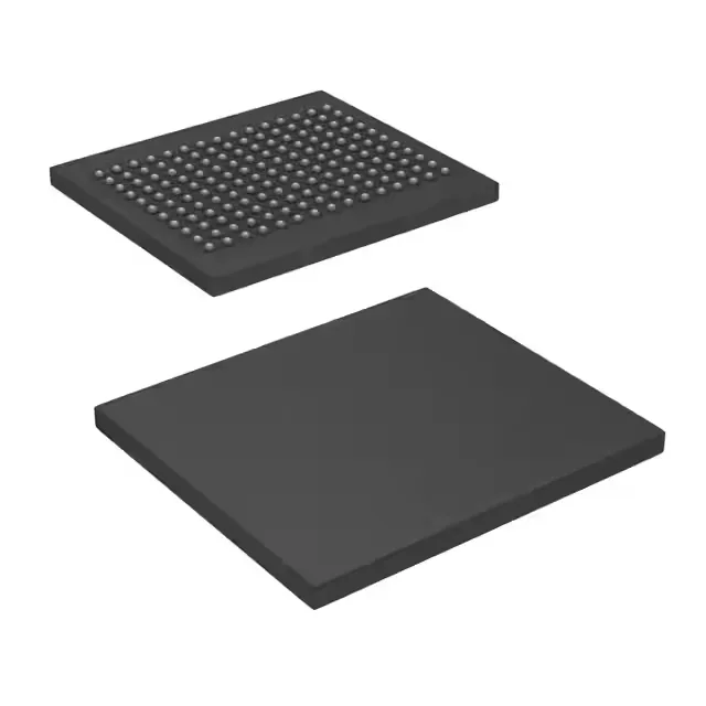
144 Mbit QDR II SRAM at 300 MHz — bandwidth budget for the line
The CY7C1613KV18-300BZXC is a 144 Mbit synchronous SRAM using the QDR II architecture, organized as 8M x 18 bits. The 300 MHz clock rate delivers a peak read bandwidth of 5.4 Gbit/s per port on the parallel bus interface — the limiting factor in a high-throughput lookup table or packet buffer is the I/O timing closure at this frequency, not the core array access.
Operates from a 1.7 V to 1.9 V core supply — the 200 mV tolerance window demands a tightly regulated rail, typically from a dedicated LDO or a point-of-load converter with less than 1% set-point error. The 165-ball FBGA package (15 mm x 17 mm body) uses a 1.0 mm ball pitch. The four-layer PCB minimum for fan-out is a board-stack constraint — the inner signal layers must carry the QDR II address and data buses with matched-length routing to maintain the 300 MHz timing budget.