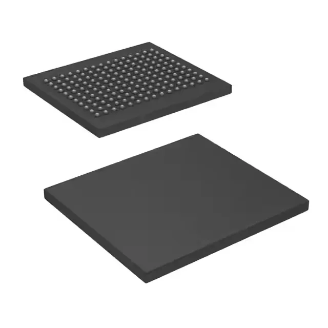
QDR II stands for Quad Data Rate, second generation — it uses separate read and write ports, each operating at double data rate, so the memory controller can issue a read and a write in the same clock cycle without bus-turnaround dead cycles. The part is organised as 8 M words by 18 bits per word — the 18-bit width accommodates a 16-bit data payload plus two parity or tag bits, common in networking lookup tables and FIFO implementations. The parallel memory interface runs at a 300 MHz clock, delivering a peak bandwidth of 1.2 G transfers per second on each port (double data rate on both read and write clocks). This limits it to controlled indoor environments — server rooms, lab equipment, central-office telecom — not outdoor or under-hood automotive use.
Because there is no pin-compatible replacement listed, a redesign or qualification of an alternative QDR II SRAM from the same or a different vendor is the only long-term fix.
The 300 MHz clock frequency is the headline performance spec. On a QDR II device, the read and write clocks each run at 300 MHz, and data is strobed on both edges, so the I/O bus operates at an effective 600 MHz data rate. The memory controller must close timing on a 1.67 ns clock period — that means tight PCB trace-length matching, controlled impedance, and clean supply decoupling right at the 165-ball FBGA footprint. The 165-ball FBGA package (15 mm x 17 mm) requires careful PCB layout for signal integrity.