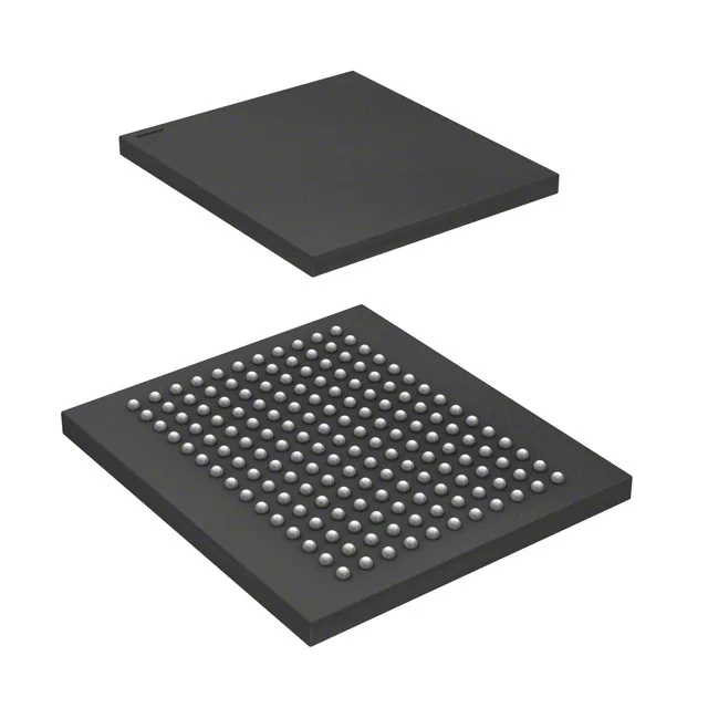
What this QDR II SRAM delivers at 250 MHz
Its 250 MHz clock rate supports back-to-back read and write transactions on separate data ports without dead cycles, which is the defining advantage of the QDR II family over conventional synchronous SRAM. The parallel memory interface keeps latency low for applications that cannot tolerate the protocol overhead of serial memory.
250 MHz clock — what it buys the system
At 250 MHz, the 18-bit-wide data bus operates at double data rate.
The base product number CY7C1612 covers the full QDR II density and speed range, so if a future speed-grade or package variant is needed, the same footprint and interface apply.
Design-in checklist for the 165-FBGA
The 165-ball FBGA (15x17 mm) requires a multi-layer PCB with at least four signal layers to route the 18-bit data buses cleanly. Supply decoupling should follow the manufacturer's recommendation for 1.8 V SRAM: a 0.1 µF capacitor per power ball pair, placed within 2 mm of the ball.