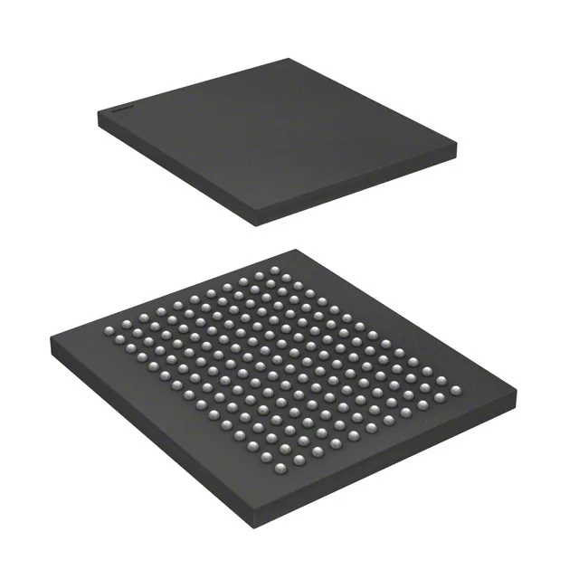
The CY7C1570V18-375BZXC: Organized as 2M x 36, it clocks at 375 MHz.
At 375 MHz, the DDR II interface toggles data on both rising and falling edges, so the effective data rate is 750 MT/s per pin. For a 36-bit-wide word, that is 27 Gbit/s aggregate bandwidth into the SRAM array. The pipelined architecture keeps the bus turning without dead cycles, which matters when you are streaming packets or filling a cache line back-to-back. The trade-off: the 165-FBGA package and 1.7 V–1.9 V supply mean the board layout needs controlled impedance and tight decoupling — this is not a part you drop into a low-speed glue-logic design.
That means the manufacturer no longer produces it, and there is no official last-time-buy window remaining. If you are still in design phase, look for a current-generation DDR II+ SRAM; if you are already in production, secure your remaining requirements through a qualified broker.
Temperature grade and handling
No lab, no bench — but if you are swapping a failed unit on a line card, the orientation is marked by pin A1 corner chamfer on the package. Hot-air rework on a 15x17 mm BGA is doable with a preheat plate, but it is not a field-swap part.