QDR II SRAM at 375 MHz — the throughput ceiling
The CY7C1543V18-375BZC is a 72Mbit synchronous SRAM built on the QDR II architecture — a double-data-rate interface that reads and writes on both clock edges, effectively doubling the data throughput per pin compared to a single-data-rate SRAM at the same clock frequency. The 375 MHz clock translates to a 750 MT/s data rate on the I/O bus, which is the bandwidth gate for high-speed networking buffers, line-card packet memories, and test-equipment capture arrays. Organised as 4M x 18 bits, the part provides 18-bit-wide data paths — common in 18-bit parity or ECC-protected memory words — and operates from a 1.7 V to 1.9 V core supply, which keeps I/O swing low enough to reduce switching noise on a dense BGA board.
Package and board-fit — 165-ball FBGA
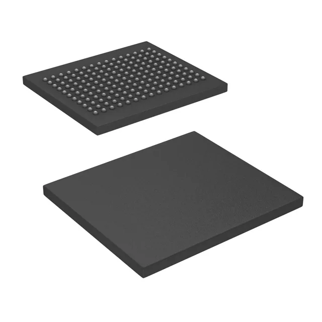
Housed in a 165-ball LBGA with a supplier device package of 165-FBGA measuring 15x17 mm, the part is a surface-mount BGA that requires a multi-layer PCB for fan-out. The 1.0 mm ball pitch is typical for this density class — a 4-layer board with blind vias can route the full 18-bit data bus and address lines without excessive layer count.
Obsolete — sourcing through surplus channels
The part is not supported for new designs; existing BOM lines must be filled through independent distribution or surplus inventory. For a line-down or repair situation, the part is available to quote against an RFQ — quantities are lot-specific and confirmed at quote time. No pin-compatible direct replacement from Infineon is documented, so a board spin or a parametric search for a QDR II SRAM in the same 165-FBGA footprint is the migration path for new builds.