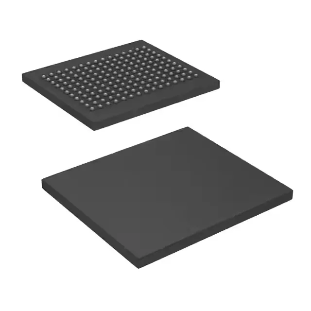
Organized as 4M x 18, it delivers a 250 MHz clock rate with read and write data transferred on both edges of the clock, effectively doubling the data bandwidth per pin compared to a conventional synchronous SRAM.
At 250 MHz, the QDR II interface delivers a peak data rate of 500 million transfers per second per I/O pin (double data rate). The 18-bit data bus yields a theoretical bandwidth of 9 Gbit/s (1.125 GB/s). This places the part in the performance tier suited for high-speed packet buffers, lookup tables, and real-time signal processing pipelines. The 165-ball FBGA package (15 x 17 mm body) keeps signal path inductance low, but the layout must maintain matched trace lengths and controlled impedance on the data and clock lines to close timing at this speed.
Commercial temperature grade — deployment boundary
If the application requires extended temperature operation, a different QDR II SRAM variant with industrial or automotive temperature grade would be needed — but no pin-compatible drop-in exists within this specific density and speed bin.
Cypress (now part of Infineon) no longer manufactures this device. No second-source or pin-compatible alternate is documented in the available records.