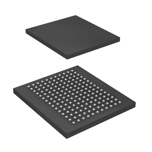
QDR II SRAM for high-throughput buffer applications
It operates at a 250 MHz clock rate, using a parallel interface with separate read and write ports to eliminate bus-turnaround dead cycles — a key advantage for network packet buffers, telecom line cards, and test equipment that need back-to-back read/write throughput without wait states.
At 250 MHz, each port delivers a peak data rate of 500 MHz equivalent (double-data-rate on the QDR bus). The 165-ball FBGA (15x17 mm) requires a four-layer minimum PCB with dedicated power and ground planes to keep signal integrity across the 18-bit data bus.
If the design can accommodate a drop-in alternative, a pin-compatible QDR II SRAM (same 165-LBGA footprint, same 1.7–1.9 V supply, same 250 MHz clock) may be available — verify the exact memory organization and timing parameters against the datasheet before substituting.
Not suitable for outdoor base stations, engine bays, or unheated enclosures without active thermal management.