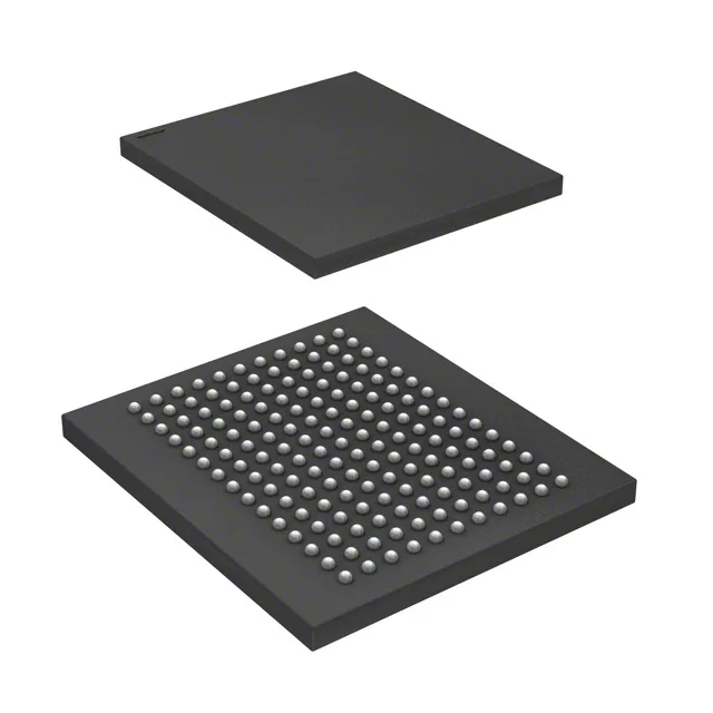
72 Mbit synchronous SRAM for high-throughput buffer and cache
The Cypress CY7C1480V33-250BZI is a 72 Mbit synchronous pipelined SRAM organized as 2M x 36 bits, clocked at 250 MHz with a 3 ns access time. Packaged in a 165-ball FBGA (15x17 mm), this part is designed for high-bandwidth data buffering, cache memory, and networking equipment where deterministic read/write latency matters.
The 250 MHz clock rate gives a 4 ns cycle time, and the 3 ns access time means the first data word appears within three clock edges after the address is presented. For a 36-bit wide data bus, this translates to a peak bandwidth of 1.125 GB/s (250 MHz × 36 bits ÷ 8). The synchronous SDR (single data rate) interface simplifies timing closure compared to DDR variants, but the 3 ns access window still demands tight PCB trace matching and controlled impedance on the address/control lines. The 2M x 36 organization is a natural fit for 32-bit or 36-bit data buses with parity or ECC — the extra 4 bits can carry byte parity without needing a second device. In a 32-bit system, the remaining 4 bits are available for tag or sideband data.
This means the manufacturer has discontinued production and no further factory orders are accepted. Any remaining stock in the distribution channel is the last available inventory. The CY7C1480 base product number family includes speed-grade variants (e.g., -200BZI at 200 MHz), but these share the same obsolete status. A form-fit-function replacement would require a different Cypress/Infineon synchronous SRAM family or a cross from a vendor like Renesas (IDT) or GSI Technology — each with its own pinout and timing characteristics that must be validated against the existing PCB layout and timing budget.
165-FBGA footprint and decoupling notes
The 165-ball FBGA (15x17 mm) package uses a 1.0 mm ball pitch. Decoupling should follow the standard practice for high-speed synchronous SRAM: one 100 nF ceramic per supply pin pair, plus a 10 µF bulk capacitor near the package. The 250 MHz clock input requires a clean, low-jitter source — a dedicated oscillator or clock generator, not a general-purpose I/O pin. The FBGA package has no exposed thermal pad; heat dissipation relies on the PCB copper planes and airflow. For high-duty-cycle operation near 250 MHz, a thermal analysis of the junction temperature against the 85°C ambient limit is recommended.