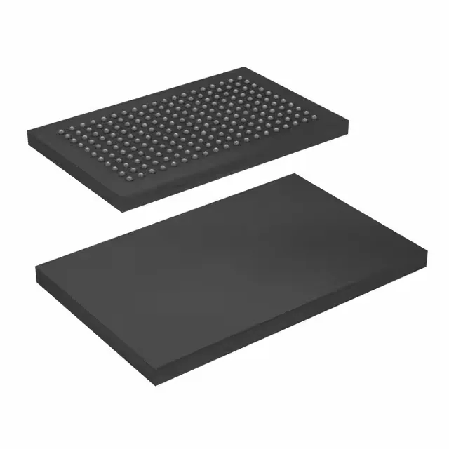
72Mbit NoBL™ synchronous SRAM for high-throughput data paths
Clocked at 200 MHz with a 3 ns access time, it keeps the pipeline full for back-to-back transactions — useful in network buffers, telecom line cards, and high-end test equipment where every bus turnaround cycle costs throughput. The 3.3V supply (3.135V to 3.6V) aligns with standard 3.3V I/O logic, and the 209-ball FBGA (14x22 mm) footprint fits a dense PCB layout.
Package and rework considerations — 209-FBGA (14x22 mm)
The 209-ball FBGA measures 14x22 mm with a 1.0 mm ball pitch typical of this density class. Pin 1 is marked by a chamfered corner on the package; verify orientation against the board silkscreen before placing, because a 209-ball BGA is not coming off cleanly if you cook it on backwards.