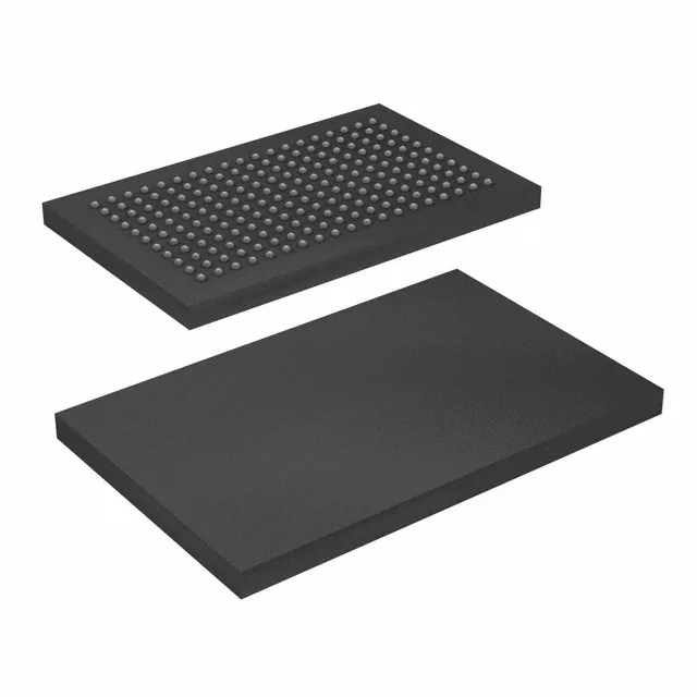
Infineon Technologies CY7C1474BV33-200BGC — Memory (DRAM / SRAM / Flash / EEPROM)

Infineon CY7C1474BV33-200BGC 72Mbit NoBL SRAM, 200 MHz

MPNCY7C1474BV33-200BGC
Obsolete

Infineon NoBL™ synchronous SRAM, CY7C1474BV33-200BGC, 72Mbit (1M x 72), 200 MHz clock, 3 ns access time, 3.135V–3.6V supply, 209-FBGA, commercial temperature.

Sourced new & surplus through independent channelsAuthenticity-screened · ESD-safe packingListing updated Jul 2026

Specifications

CY7C1474BV33-200BGC specifications
ParameterValue
SeriesNoBL™
Memory typeVolatile
MountingSurface Mount
Voltage3.135V ~ 3.6V
Frequency200 MHz
Memory interfaceParallel
Operating temperature0°C ~ 70°C (TA)
PackageTray
TechnologySRAM - Synchronous, SDR
Access time3 ns
Memory size72Mbit
Memory formatSRAM
Case209-BGA
Memory organization1M x 72

Product details

72Mbit NoBL SRAM at 200 MHz — what this part delivers

The Infineon CY7C1474BV33-200BGC is a 72 Mbit synchronous SRAM organized as 1M x 72, running at a 200 MHz clock with a 3 ns access time. It belongs to the NoBL series, eliminating the dead cycle between read and write bus turns. The part operates from a 3.135 V to 3.6 V supply and is rated for the commercial temperature range of 0°C to 70°C. Housed in a 209-ball FBGA (14 mm x 22 mm), it is a surface-mount device intended for controlled indoor environments — server rooms, central offices, lab instrumentation — not extended or industrial temperature zones.

The CY7C1474BV33-200BGC is marked obsolete by Infineon.

NoBL architecture — why it matters for throughput

NoBL (No Bus Latency) means the SRAM does not insert a dead cycle when the bus switches from read to write or write to read. In a conventional synchronous SRAM, every bus-turn incurs one idle clock; NoBL eliminates that, sustaining full 200 MHz throughput on mixed-transaction traffic. That matters for packet-processing engines where read-modify-write sequences on descriptor rings or buffer headers are the common case, not the exception.

Frequently asked questions

What is the replacement for CY7C1474BV33-200BGC?

Infineon has not listed an official direct successor for this order code. For new designs, consider Infineon's current-generation NoBL+ synchronous SRAM family in the same 209-FBGA package — verify pin compatibility and speed grade against your specific density requirement.

Where can I buy CY7C1474BV33-200BGC?

This obsolete part is sourced through independent distribution channels. Submit an RFQ for current availability and pricing — stock and lead time are confirmed at quote time.

What is the speed grade of CY7C1474BV33-200BGC?

The part is rated for a 200 MHz clock frequency with a 3 ns access time.

What is the pinout and package of CY7C1474BV33-200BGC?

The device comes in a 209-ball FBGA package (14 mm x 22 mm body). The memory interface is parallel. For the full pinout diagram, refer to the Infineon datasheet for the CY7C1474 family.