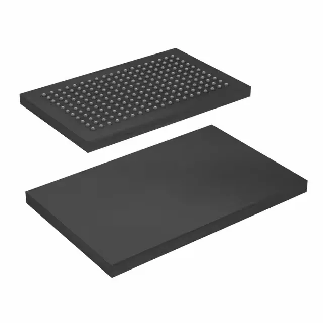
72 Mbit NoBL synchronous SRAM — 200 MHz, 3 ns access
The CY7C1474BV25-200BGIT: The NoBL (No Bus Latency) architecture eliminates dead cycles between reads and writes — the bus can switch direction on consecutive clock edges without an idle cycle, which matters for high-throughput data buffers in networking or test equipment. Supply voltage is 2.375 V to 2.625 V — a tight 2.5 V nominal rail that requires a clean regulator, not a shared 3.3 V bus.
209-FBGA package — layout considerations
Housed in a 209-ball FBGA (14x22 mm), the package demands a multi-layer PCB for fan-out. The 0.80 mm ball pitch is manageable with standard via-in-pad processes, but the tight supply tolerance (2.375 V–2.625 V) means the decoupling capacitor placement and PDN impedance need attention — a 100 nF per supply ball pair is typical for this density.