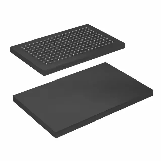
Infineon Technologies CY7C1474BV25-200BGI — Memory (DRAM / SRAM / Flash / EEPROM)

Cypress CY7C1474BV25-200BGI 72Mbit NoBL SRAM, 200 MHz, 3 ns

MPNCY7C1474BV25-200BGI
Obsolete

Cypress NoBL™ CY7C1474BV25-200BGI, 72Mbit synchronous SRAM, 1M x 72 organization, 200 MHz clock frequency, 3 ns access time, 2.375V–2.625V supply, 209-FBGA (14x22), -40°C to 85°C.

Sourced new & surplus through independent channelsAuthenticity-screened · ESD-safe packingListing updated Jul 2026

Specifications

CY7C1474BV25-200BGI specifications
ParameterValue
SeriesNoBL™
Memory typeVolatile
MountingSurface Mount
Voltage2.375V ~ 2.625V
Frequency200 MHz
Memory interfaceParallel
Operating temperature-40°C~85°C(TA)
PackageTray
TechnologySRAM - Synchronous, SDR
Access time3 ns
Memory size72Mbit
Memory formatSRAM
Case209-BGA
Memory organization1M x 72

Product details

72 Mbit NoBL synchronous SRAM — what it delivers

The NoBL pipeline eliminates the dead bus cycle between read and write operations, so back-to-back transactions run at full 200 MHz clock rate without turnaround penalties. The 3 ns access time from clock rise means the data appears on the bus within one clock edge, which simplifies timing closure in high-throughput datapaths like network buffers, test equipment, and DSP memory pools. Operating from a 2.375 V to 2.625 V supply, the part is a 2.5 V nominal device. The 209-FBGA (14x22 mm) package routes 72 data lines plus address and control in a compact footprint.

209-FBGA — what the footprint demands

The 209-ball FBGA (14x22 mm) is a fine-pitch BGA. Hand-soldering is not practical; rework requires a hot-air station with a profile matched to the package mass and a stencil for paste application. The 2.5 V supply rail must be clean — a 100 nF ceramic per supply pin group is typical, with bulk capacitance sized for the transient load of 72 I/O switching at 200 MHz.

Frequently asked questions

What is the replacement for CY7C1474BV25-200BGI?

No official replacement or successor has been recorded for this part. For a drop-in pin-compatible alternative, a cross-reference search against the CY7C1474 family in the same 209-FBGA package and 2.5 V supply is recommended. Independent distribution can also help identify functionally equivalent parts for new designs.

What is the access time of CY7C1474BV25-200BGI?

The access time is 3 ns, measured from the rising edge of the clock. This allows data to be available on the bus within one clock cycle at 200 MHz, critical for zero-wait-state memory access in high-speed systems.