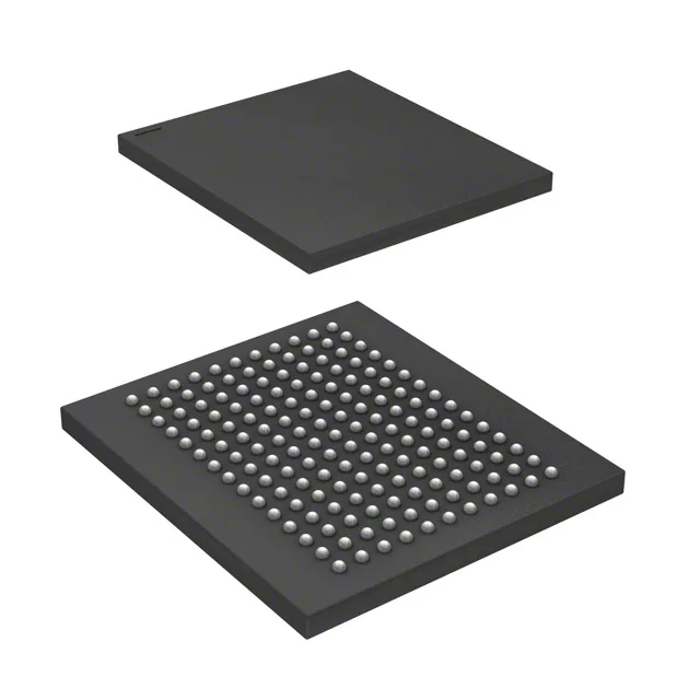
This part is designed for high-throughput, pipelined memory systems — typically network buffers, telecom line cards, or DSP scratchpads — where back-to-back read/write cycles without dead cycles are critical for sustained bandwidth.
3 ns access time — timing closure for the 200 MHz bus
A 3 ns access time at 200 MHz means the SRAM outputs valid data within 3 ns of the clock edge. That is tight: at a 5 ns clock period, the 3 ns window leaves 2 ns for the controller's input setup and trace delay. Signal-integrity simulation on the board is advisable — the 165-FBGA (15x17 mm) package has short internal bond wires, but the PCB routing from the FPGA or ASIC memory controller must keep stub lengths under 10 mm to hold the timing margin. If your system runs at 200 MHz, this part fits; if you need to relax timing, a slower clock variant (e.g., 167 MHz) in the same family would buy more margin.
The CY7C1472BV33-200BZCT is marked obsolete by Cypress (now Infineon). No longer in production, it is available only through the surplus and broker channel. If you are holding a last-time-buy (LTB) window, check the date-code traceability when sourcing from non-authorized stock — the laser etch on the 165-FBGA package should match Cypress's factory font for the week code.
165-FBGA footprint — board rework and handling
The 165-ball FBGA (15x17 mm) is a fine-pitch BGA. Reballing is possible but risky on a 0.8 mm pitch; a hot-air profile with a bottom preheat to 150°C and a top peak at 245°C is typical.