72 Mbit NoBL SRAM at 200 MHz — timing closure and bus width
The CY7C1470V25-200BZC is a 72 Mbit synchronous SRAM from Infineon's NoBL (No Bus Latency) family, organized as 2M x 36. The 200 MHz clock rate and 3 ns access time set the window the memory controller must hit for zero-wait-state reads — at this speed, board trace length matching and Vtt termination on the data bus are not optional, they are closure requirements. The 36-bit word width maps directly to a 32-bit data bus plus parity or ECC lane without packing two cycles. The parallel interface expects a 2.5 V nominal core supply (2.375 V to 2.625 V), so the rail must stay within 100 mV of 2.5 V under load to avoid setup/hold violations at the I/O pins.
165-ball FBGA and the board-level constraints
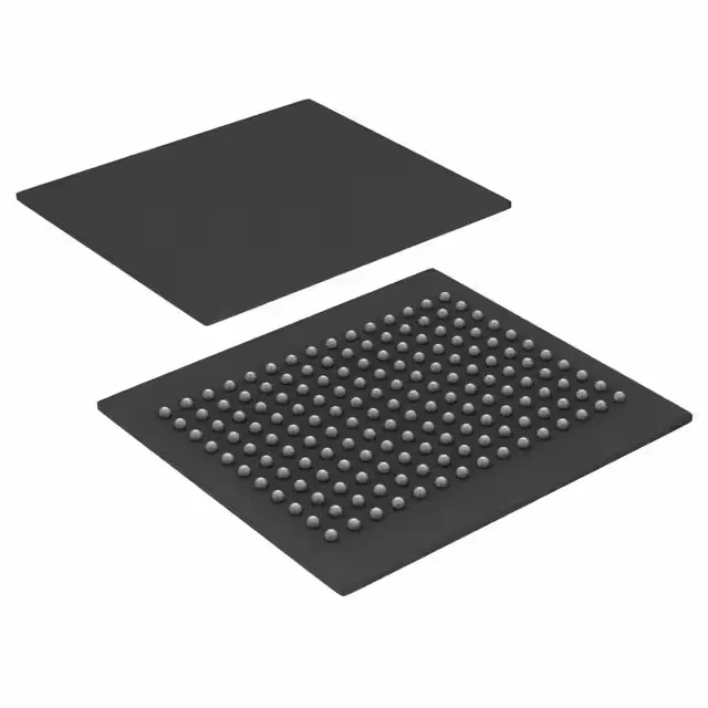
Housed in a 165-ball LBGA with a 15x17 mm body (supplier device package 165-FBGA), the BGA footprint forces a minimum four-layer PCB — the inner layers carry the 2.5 V core plane and ground, while the outer layers route the 36-bit data bus plus address and control. The tray packaging means the parts arrive in matrix trays, not tape-and-reel — pick-and-place lines need a tray feeder or a manual transfer to tape for high-volume assembly.
For a BOM that already carries this order code, the procurement path is a spot-market buy against the remaining production or repair demand. There is no pin-compatible drop-in from the same manufacturer; a board redesign would be required to migrate to a current-generation synchronous SRAM.