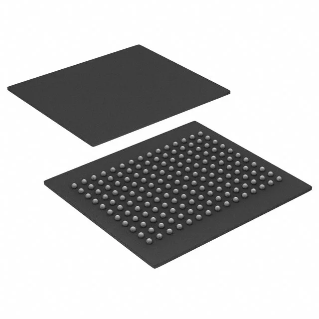
The CY7C1470BV25-200BZXC is a 72 Mbit synchronous SRAM organized as 2M x 36, clocked at 200 MHz with a 3 ns access time. The NoBL (No Bus Latency) architecture means the data bus switches between read and write without an idle cycle — the next transaction starts on the clock edge after the current one completes, which keeps the bus at full throughput for back-to-back mixed accesses. The 2M x 36 organization suits processors or ASICs with a 36-bit data word or a wide memory bus that needs to pack parity or ECC into the same chip. The 200 MHz clock rate gives a 5 ns cycle time; the 3 ns access time means the data appears on the outputs within three nanoseconds of the clock edge, leaving 2 ns of the cycle for hold and setup at the controller.
Package and board-fit — the 165-LBGA rework reality
Supply voltage is 2.375V to 2.625V — a tight 2.5V nominal rail with 5% tolerance. The core and I/O share this single supply, so the board regulator must hold regulation within that band under load transients from the SRAM's simultaneous switching outputs.
Obsolete — sourcing this part now
The 165-LBGA footprint is specific enough that a board spin would be needed for any functional replacement.