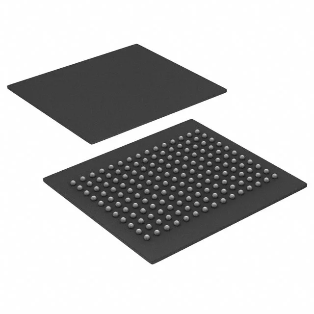
72 Mbit NoBL synchronous SRAM for high-throughput data buffers
It operates with a 200 MHz clock and delivers a 3 ns access time, enabling back-to-back read/write transactions without dead cycles on the bus.
At 200 MHz the memory supports a 5 ns cycle time. The 3 ns access time from clock edge to data valid leaves roughly 2 ns of setup-and-hold margin for the controller, which tightens the timing closure on the PCB. This part is designed for pipelined burst accesses where the NoBL architecture eliminates the turnaround cycle that conventional synchronous SRAMs insert between read and write. The 36-bit wide data bus matches a 32-bit CPU plus parity or ECC lane without needing a second device.
This exact ordering code carries an Obsolete lifecycle status. Cypress (now part of Infineon) no longer manufactures the CY7C1470BV25-200BZC in volume. The BOM line must be filled through independent distribution or surplus stock.
165-ball FBGA — layout considerations
The 165-ball FBGA (15 mm x 17 mm) uses a 1.0 mm ball pitch typical of mid-density BGA packages. The PCB requires at least four layers to route the 36 data lines plus address and control signals out of the ball array. Decoupling capacitors should sit within 5 mm of the supply balls; the 2.5 V core rail needs a clean plane with low ESL caps.