NoBL synchronous SRAM for high-throughput data paths
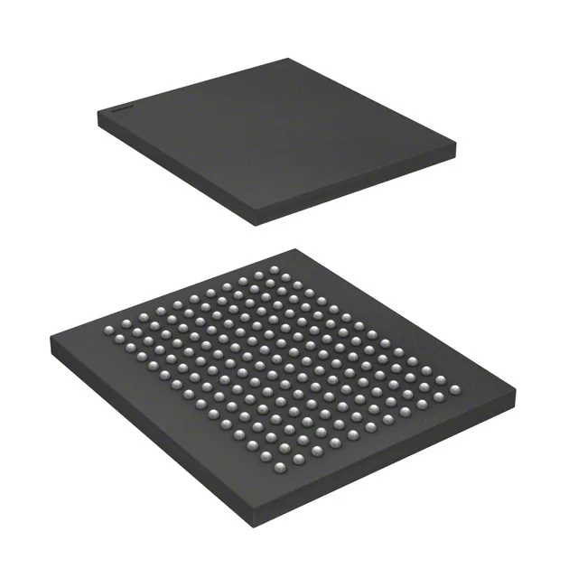
The Infineon CY7C1462KVE25-167BZI is a 36Mbit synchronous SRAM organized as 2M x 18, clocked at 167 MHz with a 3.4 ns access time. It uses the NoBL (No Bus Latency) architecture, which eliminates the dead cycle normally required when switching between read and write operations on a common I/O bus. That means back-to-back transactions at full clock rate — no turnaround penalty — which matters directly for packet buffer, cache, or FIFO replacement in networking gear, base stations, or real-time imaging pipelines where every bus cycle carries data. The part operates from a 2.5V supply (2.375V to 2.625V) and is rated over the industrial temperature range of -40°C to 85°C, so it fits outdoor telecom cabinets, factory-floor controllers, and engine-bay electronics where ambient heat or cold-soak is a given. The 165-ball FBGA package (15x17 mm) with parallel interface demands a controlled-impedance PCB and X-ray inspection on assembly — not a rework-friendly footprint, but the density and speed make that tradeoff standard for this class.
The 3.4 ns access time at 167 MHz determines whether this part meets setup/hold on a fast FPGA or ASIC memory controller. The NoBL architecture eliminates the turnaround dead cycle, so the controller never stalls waiting for the bus to float.
It is a current-production synchronous SRAM in the NoBL family.