It clocks at 167 MHz with a 3.4 ns access time, which means the memory can sustain back-to-back read or write transactions on every clock cycle without dead cycles for bus turnaround — critical for high-throughput data buffers in networking equipment, base stations, and test instrumentation where the processor or FPGA expects zero-wait-state access to a large look-up table or packet buffer. The 1M x 36 organization provides a 36-bit wide data path, which maps cleanly to a 32-bit processor bus with four extra bits for parity or ECC, or to a 36-bit FPGA interface without external byte-muxing logic. The parallel memory interface keeps latency deterministic — no serialization overhead. Supply voltage range is 2.375 V to 2.625 V, a tight 2.5 V nominal rail that requires a clean regulated supply — not a direct-from-converter rail.
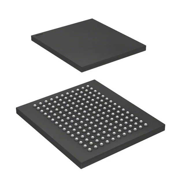
165-ball FBGA — footprint and assembly reality
For prototyping or small-run builds, factor in the cost of a PCB assembly house or a reflow oven. The package is surface-mount only, with no through-hole equivalent in this family. The 2.5 V supply rail needs low-ESR bulk capacitance to handle the transient current draw during simultaneous read-write cycles at 167 MHz.
The CY7C1460KV25-167BZCT is marked Obsolete by Cypress (now Infineon). Do not assume indefinite supply; plan a memory migration if the product has a multi-year production run ahead.