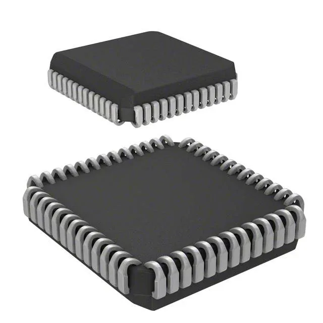
16Kbit dual-port asynchronous SRAM in a PLCC-52 footprint
The Infineon CY7C146-55JXC is a 16Kbit dual-port asynchronous SRAM organized as 2K x 8 bits, housed in a 52-lead PLCC package (J-lead, surface-mount). It provides two independent ports with separate address, data, and control lines, allowing simultaneous read or write access from two bus masters. The 55 ns access time and matched write-cycle time define the bus timing for systems that share memory between processors, DSPs, or controllers without arbitration logic overhead.
55 ns access time and dual-port arbitration
Dual-port architecture means two independent buses can access any memory location simultaneously — the internal arbitration handles same-address contention via the BUSY flag. This part is used in shared-memory designs like multiprocessor mailboxes, video frame buffers, or network packet buffers where separate controllers need a common scratchpad.
Infineon (formerly Cypress) lists the CY7C146-55JXC as obsolete. Given the obsolete status, verify date-code consistency and lot traceability when procuring from non-franchised sources; the PLCC package and J-lead form factor are distinctive and the laser etch should match Infineon/Cypress marking standards for that fab period.