What this dual-port SRAM does in the system
The Cypress CY7C146-25JC is a 16Kbit asynchronous dual-port SRAM organized as 2K x 8 bits. Its two independent ports allow simultaneous read/write access from two bus masters — typically a microcontroller and a DSP, or two processors sharing a mailbox or data buffer. The 25 ns access time means each port can complete a read or write cycle within 25 ns, which at 5 V translates to a 40 MHz equivalent bus rate for back-to-back accesses, provided the arbitration logic handles contention on the same address.
A 25 ns access time places this part in the fast-async SRAM tier. For a shared-memory design running at 25 MHz or below, the CY7C146-25JC meets a single-cycle read without wait states on most 8-bit or 16-bit buses. At higher clock rates the bus controller must insert one wait state per access.
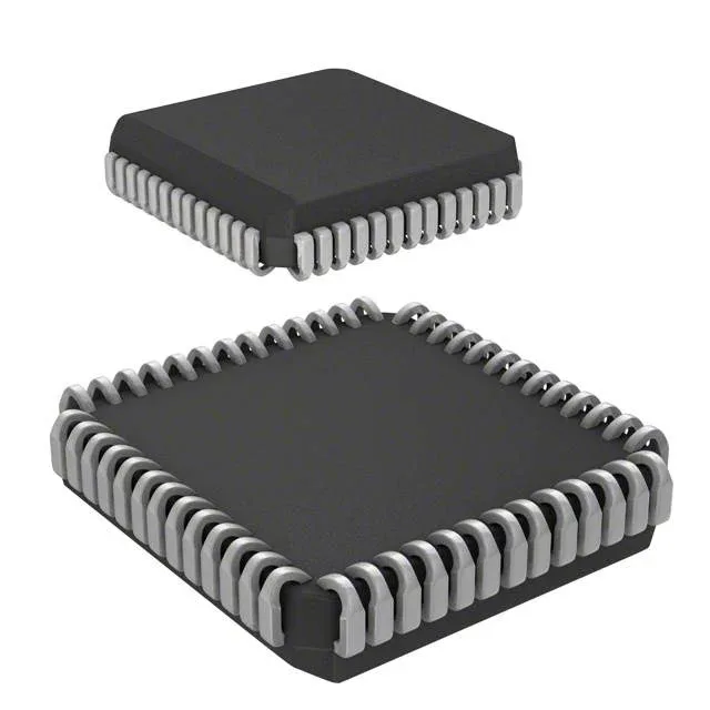
Supplied in a 52-lead PLCC with J-leads (52-LCC), the package body measures 19.13 mm square. The J-lead form factor is surface-mount but requires a PLCC socket or a footprint with the correct pad geometry — not a direct match for SOIC or QFP land patterns.
The CY7C146-25JC is marked obsolete. No last-time-buy date or successor part number appears in the record. For production or repair requiring this exact order code, procurement goes through the independent distribution channel — stock is sourced from surplus inventory, verified for authenticity and date-code freshness. There is no factory-authorized alternate; a pin-compatible drop-in from another vendor would need to be qualified on the board.