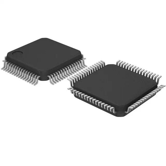
Infineon Technologies CY7C144AV-25AC — Memory (DRAM / SRAM / Flash / EEPROM)

Infineon CY7C144AV-25AC 64Kbit Dual-Port SRAM, 25ns

MPNCY7C144AV-25AC
Obsolete

Infineon Technologies CY7C144AV-25AC dual-port asynchronous SRAM, 64Kbit (8K x 8), 25 ns access, 3.0 V to 3.6 V supply, 64-LQFP, 0 to 70°C operating, Tray.

Sourced new & surplus through independent channelsAuthenticity-screened · ESD-safe packingListing updated Jul 2026

Specifications

CY7C144AV-25AC specifications
ParameterValue
Memory typeVolatile
MountingSurface Mount
Voltage3V ~ 3.6V
Memory interfaceParallel
Operating temperature0°C~70°C(TA)
PackageTray
TechnologySRAM - Dual Port, Asynchronous
Access time25 ns
Memory size64Kbit
Memory formatSRAM
Case64-LQFP
Memory organization8K x 8
Write cycle time - word, page25ns

Product details

Dual-port SRAM for shared-memory arbitration

The Infineon CY7C144AV-25AC is a 64Kbit (8K x 8) dual-port asynchronous SRAM with a 25 ns access time, designed for systems where two independent bus masters need simultaneous read/write access to a shared memory array without contention logic.

Lifecycle reality and sourcing path

No official pin-compatible successor is recorded in the lifecycle entry.

What the 25 ns access time means for bus timing

The 25 ns access time sets the window from address assertion to valid data on the output bus. For a system running a 40 MHz bus clock with a 25 ns period, the memory leaves zero margin for address decoding and trace delay — this part is best suited to slower bus architectures or where wait states are acceptable.

Housed in a 64-LQFP with a 14x14 mm body (supplier device package 64-TQFP), the CY7C144AV-25AC requires a surface-mount reflow profile compatible with JEDEC MSL level 3 or better. The 0.8 mm pitch allows two-layer PCB routing for the address and data buses, but decoupling capacitors should sit within 5 mm of each VDD pin to keep supply noise below 100 mV peak-to-peak at 3.3 V. The 8-bit wide data bus and 13-bit address bus (for 8K words) route to two separate port connectors on the board; the dual-port architecture eliminates external arbitration logic but the PCB must isolate the two port's control signals to avoid cross-talk at the 25 ns switching edge.

Frequently asked questions

What is the closest pin-compatible alternative to the CY7C144AV-25AC?

No official pin-compatible successor or direct cross-reference is recorded for this part number in the lifecycle data. For existing designs, sourcing through independent surplus channels is the available path; a board spin would be required to use a different dual-port SRAM variant.

What does the 25 ns access time mean for my system?

The 25 ns access time means the memory takes up to 25 ns from address valid to data output. This suits bus speeds up to roughly 20 MHz without wait states; at higher clock rates, the timing margin shrinks and wait states or a faster memory (e.g., 12 ns or 15 ns) would be needed.