55 ns access time — what it means for shared-memory throughput
The CY7C144-55JC is a 64Kbit dual-port asynchronous SRAM organized as 8K×8, with a 55 ns access time from address valid to data valid on either port. That 55 ns window sets the read/write cycle ceiling: the bus master must hold the address stable for the full access time before latching data, so the effective throughput is one read or write every 55 ns minimum — about 18 million accesses per second per port.
Dual-port architecture — independent port operation without arbitration logic
Both ports share the same 8K×8 memory array but each has its own address, data, and control lines. The asynchronous interface means no clock is needed — each port operates at its own pace, with the internal arbitration handling simultaneous writes to the same address via the BUSY flag. This eliminates external arbitration logic in designs where two processors or a processor and an FPGA need a shared mailbox or buffer.
68-PLCC package — reflow and socket considerations
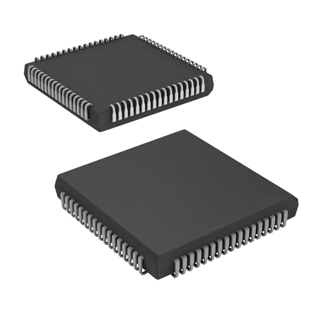
The 68-lead PLCC with J-leads (24.23×24.23 mm body) is a surface-mount package but the J-lead geometry makes visual inspection of the solder joint difficult — X-ray or a PLCC socket is the practical choice for prototyping or field service. The J-lead coplanarity tolerance is typically 0.10 mm; a stencil aperture that matches the lead footprint and a reflow profile with a 210–220 °C peak (SnPb) or 245–260 °C peak (SAC) are needed to avoid opens.
Obsolete — sourcing through independent surplus channels
Infineon (formerly Cypress) has marked the CY7C144-55JC as obsolete. No pin-compatible drop-in replacement from Infineon exists, so a board spin is required for any alternative part.
4.5V–5.5V supply — compatibility with legacy 5V buses
The 4.5V–5.5V supply range matches legacy 5V TTL/CMOS logic families. The commercial temperature grade (0°C–70°C) limits deployment to indoor, temperature-controlled equipment — not suitable for automotive, industrial, or outdoor environments without active thermal management.